Key Takeaways
- PCB prototypes are early samples of printed circuit boards that help engineers test and validate designs before mass production, reducing costly errors.
- The prototyping process involves key steps: design and layout, fabrication, and thorough testing to ensure functionality and manufacturability.
- Different types of PCB prototypes—functional, visual, and production-ready—serve specific verification needs in electronics development.
- Using PCB prototypes accelerates product development cycles, optimizes board performance, and supports regulatory certification while minimizing time and costs.
- While rapid prototyping allows for quick iteration and troubleshooting, repeated cycles and material constraints can add costs and complexity to the process.
Every electronic device begins as an idea, but turning that idea into reality requires more than just sketches and plans. This is where a pcb prototype becomes essential. These early versions of printed circuit boards allow engineers to test their designs and spot mistakes before full production starts.
By creating these test boards first, teams can make changes to layouts and fix problems without wasting time or money. PCB prototypes help check if components fit properly, if circuits work as expected, and if the board can be manufactured efficiently. This crucial step ensures the final product works exactly as planned, making it a vital part of bringing any electronic device to life.
Understanding What Is PCB Prototype
PCB prototypes are initial fabrication samples of printed circuit board designs used to test functionality before full-scale manufacturing. Engineers produce these samples in small quantities, often one to five pieces, to validate circuit layouts, check component placement, and confirm design intent aligns with system requirements. Rapid iteration with PCB prototypes helps teams identify faults in signal transmission, soldering, or layer stacking, which could lead to faults if unaddressed in mass production.
PCB prototyping commonly uses FR4, aluminum, or flexible polyimide substrates. Design teams select board material, copper thickness, and finish type based on intended application and testing scope. Quick-turn production from manufacturers like WellPCB in China offers engineers short lead times—starting from 24 hours—for single-layer, multilayer, or HDI prototypes. This time efficiency enables verification before investing resources in full-volume runs, especially for customer projects with strict deadlines or performance targets.
Applications of PCB prototypes include electronics product development, regulatory certification, and new component integration. Teams use these samples to ensure the layout meets industry standards such as IPC-A-600 for acceptability, and to screen out design flaws before mass production. WellPCB provides instant online quotes, technical support, and global delivery options that enable businesses to bring innovations to market while minimizing cost and risk during design verification.
Importance of PCB Prototyping in Electronics Development
PCB prototyping plays a key role in electronics development by giving engineers a physical sample to validate circuit designs and check practical functionality. Teams confirm electrical performance, mechanical fit, and manufacturability before large-scale production begins, reducing the probability of costly errors. By testing for issues such as signal integrity, solder joint reliability, and thermal performance, engineers optimize each board for real applications.
Faults like trace interference or incorrect component pad sizing often emerge during prototype testing. Addressing these problems at the prototype stage prevents defective mass production runs, saving time and lowering risk. WellPCB in China provides rapid prototype manufacturing with options for materials including FR4, aluminum, and flex polyimide, helping customers meet project schedules and compliance requirements.
Thorough prototyping supports design optimization, early regulatory testing, and integration of new components. Businesses minimize redesign cycles and avoid supply chain disruptions by finding problems before full-volume orders. This process ensures consistent board quality, reliable production results, and improved long-term product safety and durability. For global customers, WellPCB enables faster time to market with efficient supply solutions and high-precision sample validation.
Key Steps in the PCB Prototyping Process

PCB prototyping involves three main steps that move a board from digital design to a functional sample. Each stage covers critical processes required for manufacturability and product validation.
Design and Layout
Engineers create the schematic and board layout using CAD software, defining all circuit connections, routing paths, and component placements. A bill of materials lists every component, such as resistors, microcontrollers, and connectors. DFM checks identify physical issues—like trace width errors or spacing violations—that could disrupt manufacturing. WellPCB reviews design files in standard formats including Gerber, ODB++, and IPC-2581, ensuring data integrity and compatibility with fabrication equipment. Early DFM feedback shortens prototype cycles and prevents costly design revisions.
Fabrication
Fabrication translates digital designs into physical boards. Automated CAM tools convert design files into fabrication instructions, specifying copper layer images, drill hole locations, and solder mask areas. The process includes laminating core and prepreg layers, etching copper traces, drilling vias, and printing silkscreen markings for assembly. WellPCB uses FR4, aluminum, and flexible polyimide substrates, producing prototypes with lead times as short as 24 hours for urgent projects. Quality checks at each production step minimize defects and help maintain tight tolerances on dimensions and placement.
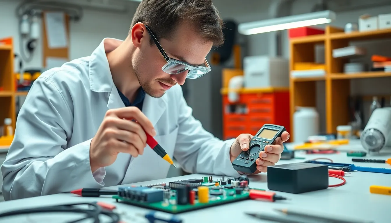
Testing and Evaluation
Testing and evaluation confirm the PCB prototype’s functionality and reliability. Technicians solder components to the board and conduct inspections for electrical continuity, short circuits, and adherence to layout specifications. Performance tests check signal integrity, impedance, and component interaction. Any detected fault—such as cold solder joints or routing errors—results in design modification and a new prototype iteration. WellPCB provides in-house electrical and functional testing for every prototype batch, certifying boards before volume manufacturing to minimize risks in production environments.
Types of PCB Prototypes
Engineers use three main types of PCB prototypes to confirm different aspects of circuit board design before large-scale manufacturing.
- Functional Prototypes
Functional prototypes test the electrical operation of a circuit board. Teams check signal integrity, power distribution, and component compatibility using these samples. WellPCB produces functional PCB prototypes so customers can verify that the design achieves required performance before moving to final production.
- Visual Prototypes
Visual prototypes allow mechanical teams to inspect physical layout and dimensions. These models help confirm fit within enclosures or assemblies. Though not as common, engineers request visual PCB samples when component placement, mounting, or connector alignment need approval.
- Production-Ready Prototypes
Production-ready prototypes closely match the intended final boards. Teams validate manufacturability, reliability, and compliance using these prototypes, making last-minute adjustments based on test results. WellPCB offers production-ready prototypes for customers needing detailed evaluation and certification before mass production.
Each prototype type supports targeted design verification. By working with PCB providers like WellPCB in China, businesses accelerate their R&D timelines, reduce error rates in production, and meet strict delivery standards through optimized prototyping solutions.
Common Applications of PCB Prototyping
PCB prototyping supports key functions in electronics product development by enabling multiple stages of testing and design validation:
- Electronics Development: Design engineers use PCB prototypes to confirm electronic device architecture before volume production. Testing with prototype boards helps verify component compatibility, signal flow, and circuit performance in early project phases. Industries such as telecommunications, automotive, and consumer electronics regularly use quick-turn prototypes from suppliers like WellPCB to meet development schedules.
- Design Validation: Project teams identify and resolve circuit design errors by assembling and evaluating prototype PCBs. Early-stage testing exposes layout mistakes, incorrect trace routing, or poor soldering joints, reducing risk prior to full manufacturing. WellPCB’s rapid prototyping services allow real-world evaluation for diverse board stack-ups, including multi-layer and flexible board designs.
- Performance Optimization: Electrical engineers use prototype iterations to refine signal integrity, electromagnetic compatibility, and power management. Multiple board versions—tested in controlled environments—let teams adjust circuit paths and layer arrangements for optimal device reliability and efficiency.
- Cost and Time Reduction: By discovering faults and inefficiencies before mass production, prototyping cuts rework time and production expenses. PCB samples enable fast troubleshooting and ensure the final product meets client and regulatory requirements.
- Low-Volume Production: Companies order prototype batches for pilot production when market volumes are uncertain or regulatory approval is pending. WellPCB in China provides small-batch runs using materials such as FR-4, polyimide, or Rogers, supporting sectors that require adaptability and short lead times.
PCB prototypes assist electronics businesses by reducing manufacturing errors, accelerating testing, and supporting flexible development cycles.
Benefits and Challenges of Using PCB Prototypes
PCB prototypes deliver rapid design validation, enabling engineers to verify circuit layouts, electrical connections, and component positioning in days instead of weeks. Teams use these models to uncover design flaws such as signal routing errors or thermal hotspots before committing to full-scale fabrication. Regular prototyping with WellPCB in China supports fast iteration and board layout refinement, helping companies address EMC compliance or manufacturability issues within strict project deadlines.
Testing real samples reduces development costs by catching errors in signal integrity or solder joint reliability at the prototype stage, limiting the risk of expensive rework during production. By accelerating time-to-market, WellPCB streamlines proof-of-concept cycles for electronics makers serving global markets.
However, repeated PCB prototype iterations create added costs, especially when advanced designs need high-frequency substrates or multilayer stackups. Constraints in prototype material choices, such as using standard FR-4 or rolled copper, may not reveal all performance aspects found in production boards. Prototype testing also involves complex inspection and validation steps, with thorough checks for electrical and mechanical performance sometimes extending project timelines. WellPCB mitigates some challenges by offering in-house DFM checks, automated quality assurance, and short delivery times, allowing designers to balance cost and test depth for each development cycle.
About WellPCB
WellPCB, based in Shijiazhuang, Hebei, China, is a leading provider of high-quality PCB manufacturing and assembly services.
Co-founded by Hommer Zhao, who also serves as the Director of Sales and Marketing, WellPCB offers comprehensive solutions, including PCB prototyping, mass production, assembly, and testing. With a commitment to delivering precision, reliability, and exceptional customer service, WellPCB supports clients in various industries, including electronics, telecommunications, automotive, and medical devices.
Contact:
Hommer Zhao, Director of Sales and Marketing, Co-founder
Phone: +86-311-86935221
Email: [email protected]
Address: 3rd Floor, Nanhai Plaza, NO. 505 Xinhua Road, Xinhua District, Shijiazhuang, Hebei, China
Website: www.ourpcb.com
Frequently Asked Questions
What is a PCB prototype?
A PCB prototype is an initial sample of a printed circuit board used to test and validate a design before starting mass production. It helps engineers check functionality, component placement, and design accuracy.
Why are PCB prototypes important in electronics development?
PCB prototypes allow engineers to find and fix design errors early, verify performance, and ensure the final product meets requirements. This reduces costly mistakes and speeds up time to market.
What materials are commonly used for PCB prototyping?
Common materials for PCB prototypes include FR4 (fiberglass epoxy), aluminum, and flexible polyimide. The choice depends on the specific application and testing requirements.
How does the PCB prototyping process work?
The process includes design and layout using CAD software, fabrication of the physical board, and thorough testing and evaluation. Each step ensures the prototype meets functionality and manufacturability standards.
What are the main types of PCB prototypes?
The main types are functional prototypes (test electrical operation), visual prototypes (check physical layout and fit), and production-ready prototypes (validate manufacturing readiness and compliance).
How does prototyping help reduce costs and time-to-market?
Prototyping uncovers design flaws early, reducing expensive errors during full-scale production and streamlining development. This accelerates the product’s path from design to market.
What problems can PCB prototyping identify?
PCB prototyping can reveal signal integrity issues, solder joint problems, incorrect component placement, and other practical faults that could lead to failures if not addressed before production.
Who uses PCB prototypes?
PCB prototypes are used by design engineers, electrical engineers, and product development teams to validate designs, refine performance, and ensure compatibility before launching full production.
Can PCB prototypes be used for regulatory and compliance testing?
Yes, PCB prototypes are often used for early regulatory and compliance testing, helping companies meet industry standards and avoid delays later in the development cycle.
What are the main challenges when using PCB prototypes?
Main challenges include added costs from repeated iterations, limited material options for advanced designs, and balancing thorough testing with budget constraints. Choosing the right prototyping partner helps address these challenges.